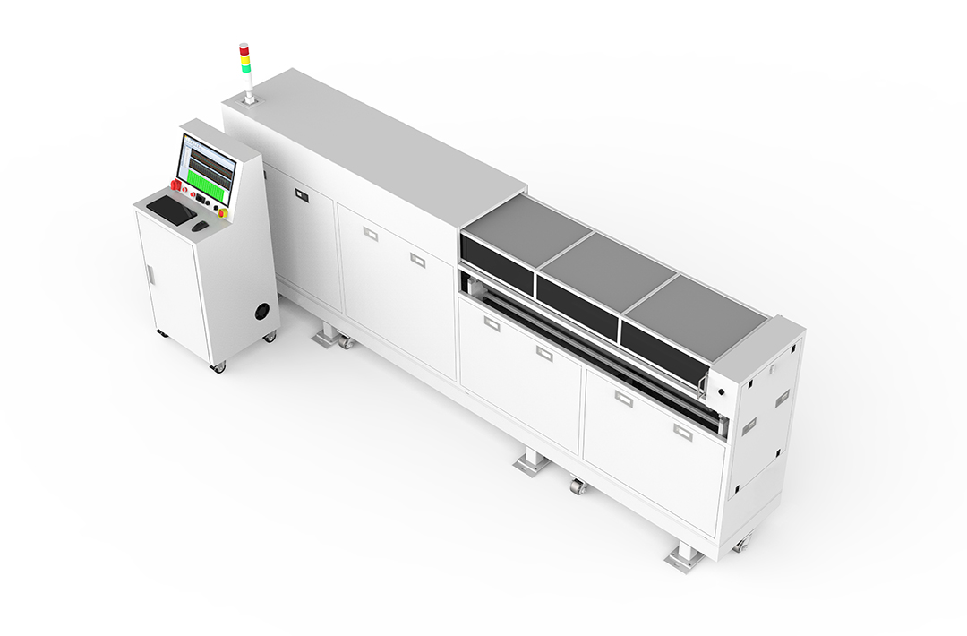
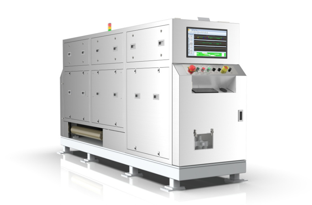
CDM integrated thickness & surface density gauge


Principles of measurement
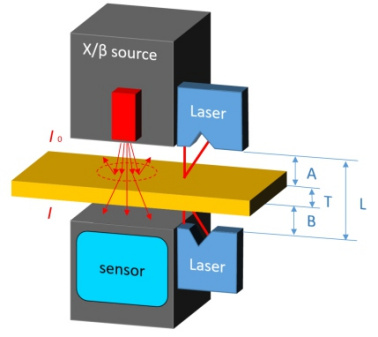
Principles of surface density measurement
X/β-ray absorption method
Principles of thickness measurement
Correlation & laser triangulation
CDM technical testing characteristics
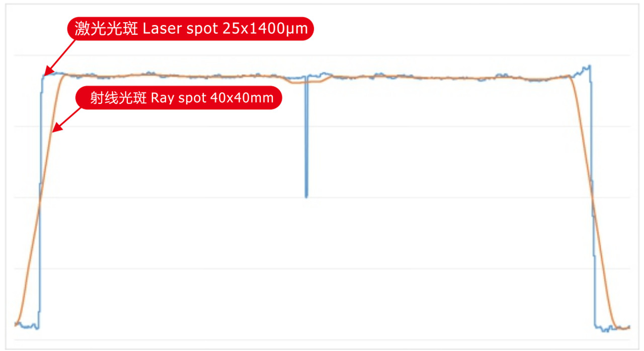
Scenario 1: There is 2 mm wide holiday/ shortage on the electrode surface and one edge is thicker (blue line as shown below). When the ray spot is 40 mm, the impact of the measured original data shape (orange line as shown below) looks smaller obviously.
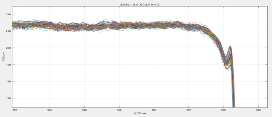
Scenario 2: profile data of dynamic thinning area 0.1mm data width
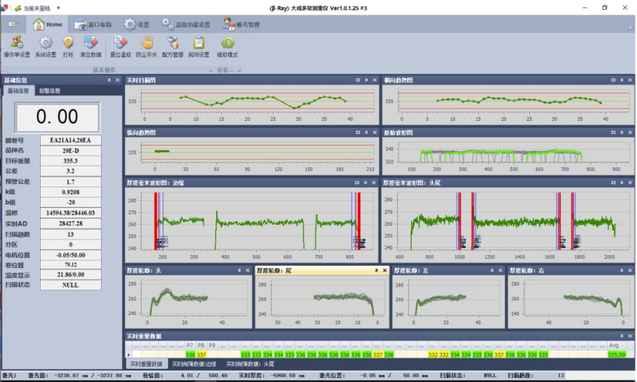
Software features
Technical parameters
| Name | Indexes |
| Scanning speed | 0-18m/min |
| Sampling frequency | Surface density: 200 kHz; thickness: 50 kHz |
| Range of surface density measurement | Surface density: 10~1000 g/m²; thickness: 0~3000 μm; |
| Measurement repetition accuracy |
Surface density: 16s integral: ±2σ: ≤±true value * 0.2‰ or ±0.06g/m²; ±3σ:≤±true value * 0.25‰ or +0.08g/m²; 4s integral: ±2σ: ≤±true value * 0.4‰ or ±0.12g/m²; ±3σ: ≤±true value * 0.6‰ or ±0.18g/m²;Thickness: 10 mm zone:±3σ: ≤±0.3μm; 1 mm zone: ±3σ: ≤±0.5μm; 0.1 mm zone: ±3σ: ≤±0.8μm; |
| Correlation R2 | Surface density >99%; thickness >98%; |
| Laser spot | 25*1400μm |
| Radiation protection class | GB 18871-2002 national safety standard (radiation exemption) |
| Service life of radioactive source |
β-ray: 10.7 years (Kr85 half-life); X-ray: > 5years |
| Response time of measurement | Surface density < 1ms; thickness < 0.1ms; |
| Overall power | <3kW |
Write your message here and send it to us